PhD thesis presented by
Dirk Lorenzen
graduate physicist
citizen of Jena, Germany
submitted to
the faculty IV - electrical engineering and computer science -
of the Technical University Berlin
for the degree of
Doctor of Technical Science - Dr.-Ing. -
accepted on the recommendation of the examination board of
Prof. Dr.-Ing. Hans-Ulrich Post (chairman)
Prof. Dr.-Ing. Dr. E.h. Herbert Reichl (examiner),
Prof. Dr. rer. nat. Thomas Elsässer (Humboldt-Universität Berlin, examiner)
filing date: january 21, 2003
date of oral presentation: september 1, 2003
publication month : october 2003
publication language : german
ISBN 3-89574-502-2
edited by Verlag Dr. Köster
The reliability of a high-power diode laser bar depends on its mechanical load during the mounting
process and on its thermal load in operation. Furthermore, the fatigue resistance of the solder
employed for packaging plays an important role for a long lifetime of the device. In this work, methods of design, calculation and measurement are presented in order to optimize the packaging of high-power diode laser bars under reliability engineering aspects. The methods of design define geometry and boundary conditions for an analytical and numerical acquisition, quantification and minimization of the problem values temperature and mechanical stress. The measurement methods serve for proving the resulting optimization within the sample - the laser bar itself. The cited methods are specially applied to the fields of micro channel cooling as well as packaging with a plastically deformable soft solder and on CTE-matched substrate suitable for hard solder mounting. |
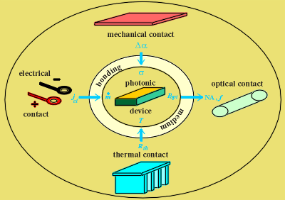
1 Introduction (2) | 1 |
2 High-power diode lasers (26) | 3 |
2.1 Design and manufacturing of diode lasers (5) | 4 |
2.2 The LI-curve of a diode laser (4) | 9 |
2.3 Optical properties of diode lasers (6) | 13 |
2.4 Reliability and ageing of diode lasers (9) | 19 |
2.5 Product development of diode lasers (1) | 28 |
3 Methodes of thermal optimisation (46) | 29 |
3.1 Cooling of diode lasers (9) | 29 |
3.1.1 Definition of thermal resistance (2) | 29 |
3.1.2 Cooling techniques for diode lasers (5) | 31 |
3.1.3 Definition of the goal of thermal optimisation(2) | 36 |
3.2 Principles of functions of micro channel coolers (6) | 38 |
3.2.1 Topology of micro channel coolers (3) | 38 |
3.2.2 Thermal calculation models for micro channel coolers (3) | 41 |
3.3 Thermal resistance of micro cooling channels (14) | 44 |
3.3.1 Convective heat transfer in micro cooling channels (4) | 44 |
3.3.2 Thermal resistance of a 2D micro channel structure (5) | 48 |
3.3.3 Thermohydraulic optimisation of micro cooling channel structures (5) | 53 |
3.4 Thermal resistance of micro channel coolers (17) | 58 |
3.4.1 Heat flux distribution and heating of coolant (5) | 58 |
3.4.2 Results of different calculation models (4) | 63 |
3.4.3 Determination of optical cap layer dimensions (3) | 67 |
3.4.4 Thermal design optimisation of laser bars (5) | 70 |
4 Methods of mechanical optimisation (44) | 75 |
4.1 Packaging technology of diode lasers (9) | 75 |
4.1.1 Mounting technology of diode lasers (2) | 76 |
4.1.2 Bonding technology of diode lasers (5) | 78 |
4.1.3 Definition of the goal of mechanical optimisation (1) | 83 |
4.2 Elastic thermomechanics of multi-layer systems (14) | 84 |
4.2.1 Basics of elasticity (6) | 84 |
4.2.2 Two-layer systems (3) | 90 |
4.2.3 Three-layer systems (5) | 90 |
4.3 Plastic thermomechanics of multi-layer systems (12) | 98 |
4.3.1 Basics of plasticity (3) | 98 |
4.3.2 Pseudo-elastistic model of plastic bonding layers (3) | 101 |
4.3.3 Stress reduction by using indium solder (6) | 104 |
4.4 Stress-reduced mounting technologies (9) | 110 |
4.4.1 Relaxative mounting technologies (2) | 110 |
4.4.2 CTE-matching mounting technologies (4) | 112 |
4.4.3 Mixed mounting technologies (3) | 116 |
5 Mechanical investigations on diode laser components (26) | 119 |
5.1 Thermomechanical measurement methods (15) | 119 |
5.1.1 Elektronic Speckle Interferometrie (5) | 119 |
5.1.2 Laser Reflexion Polarimetry (5) | 124 |
5.1.3 Photocurrent Spectroscopy (5) | 129 |
5.2 Results of mechnical investigations (11) | 134 |
5.2.1 Substrate-Induced Emitter Dicing (3) | 134 |
5.2.2 Plastically Clamped Counter Layers (3) | 137 |
5.2.3 CTE-matched Relaxative Layer Systems (5) | 140 |
6 Thermal investigations on diode lasers (20) | 145 |
6.1 Determination of thermal resistance (9) | 145 |
6.1.1 Temperature distribution in the diode laser bar (3) | 145 |
6.1.2 Measurement of heating in cw- und pulse-mode operation (3) | 148 |
6.1.3 Failure affect and estimation analysis (3) | 151 |
6.2 Results of thermal investigations (11) | 154 |
6.2.1 Cascade coolers made of copper (4) | 154 |
6.2.2 Insertion of diamond heat spreaders (4) | 158 |
6.2.3 Individually adressable emitters (3) | 162 |
7 Discussion of the results (8) | 165 |
7.1 Qualification of methods of mechanical optimisation (5) | 165 |
7.1.1 Validation of methods of mechanical measurement (2) | 165 |
7.1.2 Mechanical properties of diode laser components (3) | 167 |
7.2 Qualification of methods of thermal optimisation (3) | 170 |
7.2.1 Optimisation strategies for cooling of diode lasers (1) | 170 |
7.2.2 Thermal properties of diode lasers (2) | 171 |
8 Conclusions and outlook (1) | 173 |
APPENDIX (24) | 175 |
Material parameters (3) | 176 |
Symbols (6) | 179 |
Abbreviations (2) | 185 |
References (7) | 187 |
Publications (2) | 194 |
Acknowledgements (2) | 196 |
Curriculum vitae (1) | 198 |
High power diode laser bars are electro-optic gallium arsenide based devices with a quite high
lateral extension of about 10 mm. Their reliability depends essentially on their temperature
during operation and mechanical load during packaging. Furthermore, reliability is correlated
with migration resistance of the solder used for mounting.
It is the goal of a reliability-guided optimization of high power diode laser bar packaging
to reduce operation temperature and packaging-induced stresses, preferably using a fatigue
resistant hard solder.
The most effective cooling for laser bars is micro channel cooling that employs water as coolant (the so-called active cooling). In the present work, two different models to calculate the thermal resistance of micro channel coolers have been developed - a first one completely analytic and a second one, that is based on a simplified method of two-dimensional finite elements. In a more detailed way, the heat flow path into the side of micro channel facing the laser bar has been taken into account, as well as - for the first time - the heat flow path into the supply channels which are located at the side of the micro channels turned away from the laser bar. Especially the latter path promises a considerable reduction of the thermal resistance. This is underlined by the experimental values of standard copper micro channel coolers: The measured 0,5 K/W coincide - within measurement errors - with those of the theory. With the aid of the analytic thermal resistance calculation model, at first, the size, form and numbers of channels has been optimized. In a further stage, the channel structure optimization has been directed to the special requirements of active cooling in user-friendly diode laser stacks. In order to do so, position, orientation and order of channels with respect to a serial water flux through them has been considerated. The resulting, very effective cascade coolers have been for the first time developed and characterized in the framework of this study. As a supplement to reducing the thermal resistance of micro channel structures, an optimization procedure for the thickness of the heat spreading cap layer between laser bar and micro channels has been proposed. For heat spreading layers made of diamond, packages with integrated micro channels and a central position of the laser bar on the heat spreader have been realized. Thermal resistances of 0,2 to 0,25 K/W have been measured. The combination of both types is promising thermal resistances of less than 0,15 K/W. Moreover, two methods for thermal optimization of a laser bar structure fit to the existing cooling conditions have been developed. By this, for the first time, a general analytical optimization tool to reduce the heating of laser diode bars has been created. Standardly laser diode bars are mounted by a highly plastic soft solder on copper heat sinks in order to reduce mechanical stresses arising during the bonding process as a result from the CTE-mismatch of the bonding partners. Before the beginning of this work, no calculations or measurements of stress distributions in plastically mounted laser bars were known. An analytical solution for the stress distribution along the laser bar width has been derived by an ex-tension of the SUHIR model for the case of a plastic solder between heat sink and laser bar. The shape of the resulting stress distribution function is hyperbolic. By introducing a pseudo-elastic Young's modulus a simplified method of 2D finite elements could be applied. The results from this calculation fit very well with those obtained from 3D elasto-plastic FEM simulations. The stress distribution obtained from these calculations exhibits a linear rise of stress from the borders of the laser bar to the center - this is typical for purely plastic bondings. This nearly triangular shape of has been proven by stress measurements. In the present work, two novel experimental setups for measuring stress distributions in laser bars have been realized: photocurrent spectroscopy (developed by the Max-Born-Institut in Berlin) and laser reflection polarimetry. The novelty of the latter technique resides in a scanned recording of the stress amount integrated along the resonator direction. While the calculation using the pseudo-elastic Young's modulus promises maximum stress values of 70 MPa in the laser bar, photocurrent spectroscopy provides values around 60 MPa. This is a good agreement between theory and experiment. The result emphasizes a plastically induced stress reduction down to 40 % of the amount that would arise without a plastic bonding layer. In order to achieve the goal of realizing a stress-reduced package combined with a high amount of thermally highly conductive diamond close to the laser bar, several packaging techniques have been conceived, optimized, realized, proven and evaluated. For the first time, the techniques of substrate induced dicing, plastically clamped counter layers and relaxed CTE-matched layer systems have been presented. The determination of the optimal layer thicknesses in the latter technique has been supported by measurement of thermally induced deformations using electronic speckle pattern interferometry. All three packaging techniques enable a location of the laser bar in a distance of less than 35 µm from a heat spreading diamond substrate and - in comparison with standard techniques - a considerably reduced packaging stress of less than 10 MPa in some cases. None of these techniques, however, could fulfill all three requirements of optimized cooling, biaxial stress freeness over the whole laser device and hard solder bonding. Based on the techniques developed in this work, this goal should be achieved in the future. |